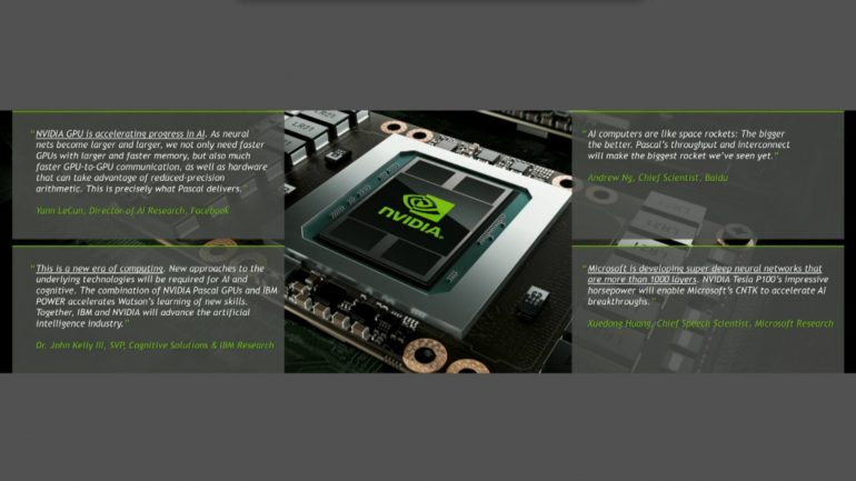
After unveiling the Tesla P100 HPC board NVIDIA has made one step forward and has announced the GP100 GPU, which is the first graphics processing unit to come to us from the Pascal generation the company has been working on in the past year or two.
The new chip does not disappoint one bit – it is made with 16 nm FinFET technology and it includes 15.3 billion transistors in a die that is 610 mm² large. This is also the first NVIDIA chip to include HBM memory but NVIDIA jumps right into HBM2 technology, so GP100 features the more advanced second generation HBM memory. In addition GP100 supports dual-link NVLink technology for up to 160 GB/sec of memory bandwidth, new Unified Memory and Compute Preemption algorithms and more. NVIDIA says GP100 will bring significant FP64 performance improvements compared to the older GK110 (Kepler) and GM200 (Maxwell) GPUs. Inside the GP100 chip includes 60 SMX units with each one of them having 64 stream processors and 4 texture units for a total of 3840 stream processors and 240 TMUs. The hardware is split between FP32 and FP64 units in a ratio of 2:1. Additionally video cards based on GP100 will feature up to 16 GB of HBM2 memory, and a 4096-bit memory bus (made of eight 512-bit memory controllers). The memory will provide 720 GB/sec of memory bandwidth, which means it will run at 700 MHz.
The first products on GP100 will appear this summer.
Source: NVIDIA

