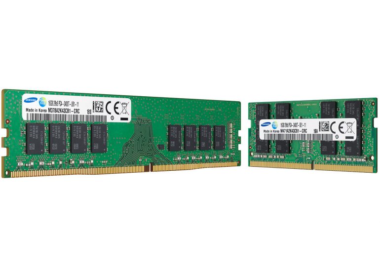
One of the largest producers of computer memory – Samsung – has announced its transition to mass production of 10 nm 8-gigabit DDR4 DRAM memory chips and modules that are based on them. The new tech achievement will allow Samsung to produce DDR4 memory at a lower cost, while providing higher density memory modules that need less power to operate.
“Samsung’s 10nm-class DRAM will enable the highest level of investment efficiency in IT systems, thereby becoming a new growth engine for the global memory industry,” said Young-Hyun Jun, President of Memory Business, Samsung Electronics. “In the near future, we will also launch next-generation, 10nm-class mobile DRAM products with high densities to help mobile manufacturers develop even more innovative products that add to the convenience of mobile device users.”
The adoption of 10 nm 8 Gb DDR4 memory greatly improves the wafer productivity of 20 nm 8 Gb DDR4 DRAM by more than 30 per cent and in addition to this the new memory reaches a data transfer rate of 3200 megabits per second (Mbps), which is more than 30 per cent faster than the 2400 Mbps rate of 20 nm DDR4 DRAM. Moreover the memory modules made on 10 nm technology need 10 to 20 per cent less power, compared to their 20 nm process-based equivalents, which will further lower the overall power consumption of future computer systems. To achieve this Samsung has overcome different difficulties in DRAM scaling by using current argon fluoride immersion technology, which is free from the use of extreme ultra violet equipment. This is not a small feat by itself.
The adoption of a 10 nm production process for its DDR4 memory production will allow Samsung to introduce new DDR4 memory modules with capacities from 4 GB for notebooks to 128 GB for enterprise servers.
Source: Samsung
